TRE-3S
Prices starting at $4,500

Standard Features:
Tracking: Total 874 channels: all-in-view satellite tracking, GPS L1/L2/L2C/L5, Galileo E1/E5A/E5B/AltBoc/E6, GLONASS L1/L2/L3, BeiDou B1/B1C/B2/B3, QZSS L1/L2/L5/L6 (L61/L62), IRNSS L5, L-Band, SBAS L1/L5, Spectrum Data Output, Spoofing Detection, Advanced Multipath Reduction, In-band Interference Rejection, GLONASS .2mm Dynamic Calibration, Heading Determination, Attitude Determination, Fast acquisition channels
Data: 20 Hz update & RTK rate for real time position and raw data (code and carrier), Hardware Viterbi decoder, RTCM SC104 versions 2.x and 3.x Input/Output, NMEA 0183 versions 2.x and 3.0 Output, Code Differential Rover, Code Differential Base, Geoid and Magnetic Variation models, RAIM, Different DATUMs support, Output of grid coordinates, IEEE 1588 Master Clock, RINEX/BINEX data output; Reed-Solomon and LDPC decoders, 64 GB of onboard memory for data storage
I/O: Two high speed RS232 serial ports (up to 460.8 Kbps), Two high speed configurable RS232/RS422 serial ports (up to 460.8 Kbps), Two high speed USB 2.0 device port (480 Mbps), Full-duplex 10BASE-T/100BASE-TX Ethernet port, Two CAN 2.0 A/B ports, IRIG timecode output, Two 1-PPS outputs synchronized to GPS, GLONASS or UTC, Two Event Marker inputs, External Frequency Input/Output, MinPad interface: Four external LED drivers, ON/OFF control and External Command inputs, Four Configurable Logic-Level GPIO ports
Optional Features:
Tracking: QZSS L6 (LEX)
Data: 200 Hz Update Rate, 200 Hz RTK Rate, QZSS L6 (LEX) Data, IRNSS S-band, Conformal coating
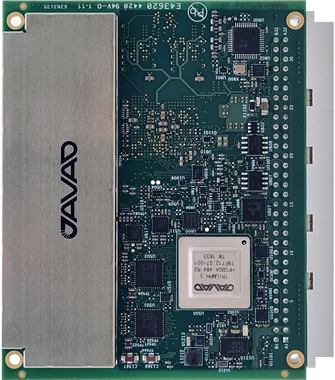


Specifications:

Physical

  • Dimensions: 100x80 mm
  • Weight: 87 g
  • Digital connector: 64-pin DIN41612 type B Right Angle, AMP p/n 536052-5
  • RF connectors: MMCX Jack, edge mount, AMPHENOL, p/n 908-2210

Electrical

  • On-board power supply accepts any unregulated voltage between +4.5 to +40 Volts
  • The central pin of the antenna connector outputs +5 VDC to power LNA. The sourced current is 0.12A max.
  • Power consumption: 4.7 Watt

Description I/O Signal Name Pin # Pin # Signal Name I/O Description
Power Ground   PGND A1 B1 PGND   Power Ground
+4.5 to +40 VDC Power Input I PWR_IN A2 B2 PWR_IN I +4.5 to +40 VDC Power Input
Factory use only, must be left open   FUO A3 B3 COMMSW# I Active Low Command Input (FN Button)*1
Selects between host and peripheral modes *2I USB1_ID A4 B4 KA_PWR I Keep-Alive Power input for Real-Time Clock (+4.5 to +40 VDC, 10μA typ)
External LED Control *3 O LED2_RED A5 B5 LED1_RED O External LED Control *3
External LED Control *3 O LED2_GRN A6 B6 LED1_GRN O External LED Control *3
Signal Ground   GND A7 B7 USB1_PWR I USB port Power Input line
USB port D- line*2I/O USB1_D- A8 B8 USB1_D+ I/O USB port D+ line*2
Serial port A TXD lineO TXDA A9 B9 CTSA I Serial port A CTS line line
Serial port A RXD lineI RXDA A10 B10 RTSA O Serial port A RTS line line
Serial port C: RS232 TXD line or RS422 TX- line O TXDC/TXC- A11 B11 CTSC/RXC+ I Serial port C: RS232 CTS line or RS422 RX- line
Serial port C: RS232 RXD line or RS422 RX- line I RXDC/RXC- A12 B12 RTSC/TXC+ O Serial port C: RS232 RTS line or RS422 TX- line
Serial port D: RS232 RTS line or RS422 TX+ line O RTSD/TXD+ A13 B13 TXDD/TXD+ O Serial port D: RS232 TXD line or RS422 TX- line
Serial port D: RS232 CTS line or RS422 RX+ line I CTSD/RXD+ A14 B14 RXDD/RXD- I Serial port D: RS232 RXD line or RS422 RX- line
Signal Ground   GND A15 B15 USB2_PWR I USB port Power Input line*2
USB port D- line*2I/OUSB2_D- A16 B16 USB2_D+I/OUSB port D+ line*2
Serial port B TXD line O TXDB A17 B17 CTSB I Serial port B CTS line
Serial port B RXD line I RXDB A18 B18 RTSB O Serial port B RTS line
CAN1 port CAN-H line I/O CAN1H A19 B19 CAN1L I/O CAN1 port CAN-L line
CAN2 port CAN-H line I/O CAN2H A20 B20 CAN2L I/O CAN2 port CAN-L line
Factory use only, must be left open   FUO A21 B21 USB2_ID I Selects between host an peripheral modes *2
Signal Ground   GND A22 B22 1PPSA O 1 Pulse Per Second output A *4
Signal Ground   GND A23 B23 1PPSB O 1 Pulse Per Second output B *4
Signal Ground   GND A24 B24 EVEBTA I Event input A *5
Signal Ground   GND A25 B25 EVEBTB I Event input B *5
Configurable Logic-Level I/O 0 line I/O GPIO0 A26 B26 GPIO1 I/O Configurable Logic-Level I/O 1 line
Configurable Logic-Level I/O 2 line I/O GPIO2 A27 B27 GPIO3 I/O Configurable Logic-Level I/O 3 line
Signal Ground   GND A28 B28 RESET_IN# I Active Low Reset input *6
Ethernet port TX+ line O LAN_TX+ A29 B29 LAN_TX- I Ethernet port TX- line
Reserved   - A30 B30 LAN_LED O Ethernet port control fot external LED
Ethernet port RX+ line I LAN_RX+ A31 B31 LAN_RX- I Ethernet port RX- line
Active Low input for ON/OFF switch *8 I ONOFFSW# A32 B32 IRIG_OUT O IRIG port output line *7
  • *1 Active Low input from the FN button of the MainPad. Must be left open if not used.
  • *2 Simultaneous use of two USBs in HOST mode is not supported.
  • *3 LED1_GRN and LED1_RED are used to control the STAT LED of the MinPad. LED2_GRN and LED2_RED are equivalent to the REC LED of the MinPad. The output is a +3.3V driver in series with 100 Ohm resistor for each LED. LEDs should be with common cathode.
  • *4 Voh>1.8V at 50 Ohm load.
  • *5 Internal pull-up 5 kOhm to +3.3V.
  • *6 Connect to ground to active. Internal pull-up 2 kOhm to +3.3V.
  • *7 AM sine-wave signal; 2.1Vp-p (Mark), 0.7Vp-p (Space).
  • *8 Active Low input which is equivalent to ON/OFF button of the MinPad. After abnormal turn off because of external power failure, the boards turn on automatically when external power is restored.

Environmental

  • Operating Temperature: -40°C to +80°C
  • Storage Temperature: -40°C to +85°C
  • High shock and vibration resistance